What’s new with the Memory Protection Unit (MPU) in Cortex-M23 and Cortex-M33?
ARM Cortex-M23 and Cortex-M33 processors, announced recently at ARM TechCon 2016, both integrate a new Memory Protection Unit (MPU). This optional MPU is based on an updated ARM Protected Memory System Architecture (PMSAv8), which brings more flexibility and ease of programming compared to its predecessors found in Cortex-M0+, Cortex-M3, and Cortex-M4. The change in programming model, however, does require that existing MPU setup software written for Cortex-M0+, Cortex-M3, and Cortex-M4 be updated. Before we look at what’s changed, let’s quickly review what an MPU is, and why it is so useful.

ARM Cortex-M23 and Cortex-M33 processors, announced recently at ARM TechCon 2016, both integrate a new Memory Protection Unit (MPU). This optional MPU is based on an updated ARM Protected Memory System Architecture (PMSAv8), which brings more flexibility and ease of programming compared to its predecessors found in Cortex-M0+, Cortex-M3, and Cortex-M4. The change in programming model, however, does require that existing MPU setup software written for Cortex-M0+, Cortex-M3, and Cortex-M4 be updated. Before we look at what’s changed, let’s quickly review what an MPU is, and why it is so useful.
What’s an MPU?
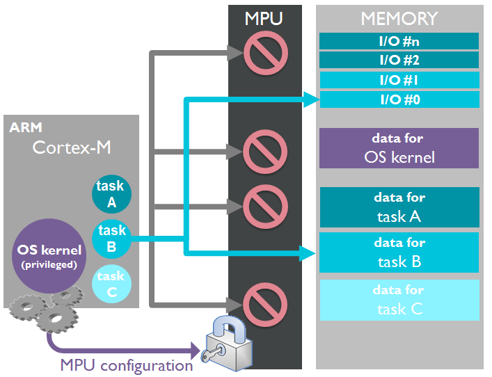
The MPU is a programmable unit inside the processor that allows privileged software to define memory access permissions and memory attributes to different regions within the 4GB memory space. All memory access is monitored by the MPU, which can trigger a fault exception if unauthorized access is attempted. The MPU adds robustness to embedded systems in many different ways. It can prevent stack overflows in one task from corrupting memory belonging to another task. It can define regions of memory where access is never allowed by instruction fetches, thus preventing any potential malicious code from being executed from those regions. It can secure regions of RAM/SRAM from accidental corruption by defining those regions as read-only. It can also define regions of memory as “shareable” when multiple masters in the system have access to that region. By being shareable, the system is required to ensure coherency for that region among its masters.
Figure 1: Example MPU usage: preventing task B from corrupting memory region belonging to OS or other tasks.
What’s new in PMSAv8 MPU?
Using Start and Limit (end) address to define memory regions simplifies memory region definition and leads to a more efficient use of available memory space. In previous PMSAv7 MPUs, memory regions had to be defined by a base address and a size, which was limited to 2n byte sizes. When a region of arbitrary size was required, several smaller sub-regions had to be used to reach the target size. (See Figure 2 below.)
Figure 2: PMSAv8 no longer has 2n Byte size requirement on memory regions
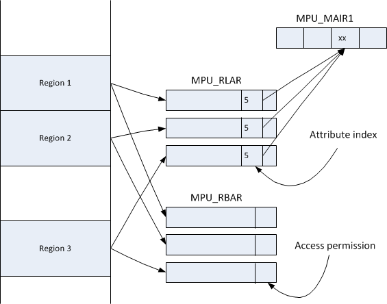
PMSAv8 MPU also brings new memory attribute indirection registers (MPU_MAIR) that make it easier for multiple regions to share the same attribute, while at the same time maintaining their own access permissions. For example, multiple SRAM regions can have the same cache-related memory attributes, but some regions can be set to be ‘execute never’ (XN), while another can be accessible by both instruction fetches and data read/write. The memory attribute index field in MPU_RLAR register for each region indicates which of the eight memory attributes defined in the attribute indirection register (MPU_MAIR) to use.
Figure 3. Same memory attribute assigned to regions 1, 2, and 3.
So there is definitely a new programming model for the PMSAv8 MPU that programmers need to be aware of. There are also more number of regions allowed for any implementation of Cortex-M23 or Cortex-M33. There can be 0, 4, 8, 12, or 16 regions definable by the MPU. Previously, the number of regions allowed on a Cortex-M0+, Cortex-M3, or Cortex-M4 was either 0 or 8.
Equally important to realize is the fact that all MPU registers are banked. If TrustZone is enabled, there is a set of MPU registers for the Secure state, and a mirror set for the Non-secure state. Non-secure code can access Non-secure MPU registers and Secure code can access Secure MPU registers. In addition, Secure code can access Non-secure MPU registers at their aliased address. The new MPU registers on Cortex-M23 and Cortex-M33 are shown in Table 1.
|
Register |
Description |
|
MPU_TYPE |
MPU Type Register |
|
MPU_CTRL |
MPU Control Register |
|
MPU_RNR |
MPU Region Number Register |
|
MPU_RBAR |
MPU Region Base Address Register |
|
MPU_RBAR_An |
MPU Region Base Address Register Alias n. n={1..3} |
|
MPU_RLAR |
MPU Region Limit Address Register |
|
MPU_RLAR_An |
MPU Region Limit Address Register Alias n. n={1..3} |
|
MPU_MAIRn |
MPU Memory Attribute Indirection Register n. n={1,2} |
Table 1. List of MPU registers in Cortex-M23 and Cortex-M33
CMSIS-CORE updated to support new MPU
The latest Cortex CMSIS v5 supports the new MPU programming model by including new CMSIS-CORE APIs for programming MPU registers - there is also an example MPU setup code that can be used. See Memory Protection Unit for ARMv8-M based platforms for more details on these CMSIS-CORE API functions. Care should be taken when initializing MPU registers by using memory barrier instructions to ensure that any write to MPU registers is complete before allowing subsequent memory accesses. The use of DMB, DSB, and ISB instructions are recommended.
As a reminder, DMB (Data Memory Barrier) is used before disabling the MPU prior to initializing MPU registers. DMB ensures that any outstanding transfers are complete before writing to the MPU control register to disable the MPU. Once programming of MPU registers is done and the MPU is re-enabled, DSB (Data Synchronization Barrier) is used to ensure that the subsequent ISB instruction is executed only after the write to the MPU control register is completed. And finally, the ISB (Instruction Synchronization Barrier) is used to ensure the processor pipeline is flushed and subsequent instructions are re-fetched with the updated MPU settings.
Summary
The MPU brings more robustness to embedded systems by providing memory access permission control, and it enables system behaviour to be optimized by providing memory attributes control. The MPU enhancements in ARMv8-M architecture enable more flexibility in region size definitions and also allow separate MPU configurations between software in Secure and Non-secure domains, enabling a wider range of application use cases.
Re-use is only permitted for informational and non-commerical or personal use only.


